Please Log In for full access to the web site.
Note that this link will take you to an external site (https://shimmer.mit.edu) to authenticate, and then you will be redirected back to this page.
This lab is split into three parts, all of which explore concepts in sequential logic design:
- Build a button-press counter, and display the current count on your output LEDs in raw binary.
- Get multiple digits rendering on the seven-segment display. Because of the circuitry, this will require a sequential logic circuit to take advantage of our relatively slow visual responsiveness. Prove this is working by rendering your button count from the previous section with it.
- Finally, read in a keyboard's PS/2 output, feed it into a shift buffer, and display the last four PS/2 code bytes on the seven-segment display!
Just like last time, create a new project folder. Repeat the file structure we used in Lab 01, with the following folders:
src: to hold all your Verilog files that will be synthesized (built on the FPGA)xdc: to hold the XDC file for mapping and activating pinssim: to hold all Verilog files that are for simulating/testbenchingobj: to hold all output files from your Vivado builds.
Take the generic build tcl script and place it in the root of your lab folder. Alternatively, if you are using lab-bc.py, download the latest version from the Vivado documentation page and place it in the root of your lab folder - we've changed a few things since lab 1.
Put a copy of the default xdc file in your xdc folder.
Create a top level file called top_level.sv in src, and set up things so the following inputs and outputs are made available for your top level module (by modifying/uncommenting the common .xdc file you just downloaded):
clk_100mhz: Uncomment both related lines to this at the top of the xdcled: All sixteen green LEDsca,cb,cc,cd,ce,cf,cg: The cathodes common to all eight seven-segment digitsan[7:0]: The selection anodes for each seven-segmentbtnc: This button will be debounced and countedbtnd: We'll use this button as a global resetps2_clk: The PS/2 clock lineps2_data: The PS/2 data line
As a starting skeleton for your top_level.sv we've provided the following code:
`timescale 1ns / 1ps
`default_nettype none

module top_level( input wire clk_100mhz,
                  input wire btnd,btnc,
                  input wire ps2_clk,
                  input wire ps2_data,
                  output logic [15:0] led,
                  output logic ca, cb, cc, cd, ce, cf, cg,
                  output logic [7:0] an
                );

  /* have btnd control system reset */
  logic sys_rst;
  assign sys_rst = btnd;

  /* how many button presses have we seen so far?
   * wire this up to the LED display
   */
  logic [15:0] btn_count;
  assign led = btn_count;

  /* this should go high for one cycle on the
   * rising edge of the (debounced) button output
   */
  logic btn_pulse;

  /* debouncer for the button. we wrote this
   * in lecture together.
   * TODO: make a variable for the debounced
   * button output, and feed it into your edge
   * detector
   */
  debouncer btnc_db(.clk_in(clk_100mhz),
                  .rst_in(sys_rst),
                  .dirty_in(btnc),
                  .clean_out(/* your variable here */));

  /* TODO: write your edge detector for part 1 of the
   * lab here!
   */

  /* the button-press counter.
   * TODO: finish this during part 1 of the lab
   */
  simple_counter msc( .clk_in(clk_100mhz),
                      .rst_in(sys_rst),
                      .evt_in(btn_pulse),
                      .count_out(btn_count));

  /* TODO: you'll finish this in part 2 of the lab. this will
   * render the button count and the four PS/2 buffer
   * values in parts 2 and 3 respectively
   */

  /* For part 1 of the lab, you won't use this yet! So leave
   * this commented out unless you want errors hehe
   */

  /*
   * seven_segment_controller mssc(.clk_in(clk_100mhz),
   *                               .rst_in(sys_rst),
   *                               //.val_in({ps2_buffer[3], ps2_buffer[2], ps2_buffer[1], ps2_buffer[0]}),
   *                               .val_in(btn_count),
   *                               .cat_out({cg, cf, ce, cd, cc, cb, ca}),
   *                               .an_out(an));
   */

  /* Delete this once you're done with part 2 of the lab */
  assign {cg, cf, ce, cd, cc, cb, ca} = 8'b0;
  assign an = 8'b1111_1111;

  /* pull inputs from the ~15KHz PS/2 domain
   * our FPGA's 100 MHz clock domain. this code
   * acts as a 'synchronizer' - we will talk more
   * about this later. for now, don't change it
   */
  logic [1:0] ps2b_c;
  logic [1:0] ps2b_d;

  always_ff @(posedge clk_100mhz)begin
    ps2b_c[0] <= ps2_clk;
    ps2b_d[0] <= ps2_data;
    ps2b_c[1] <= ps2b_c[0];
    ps2b_d[1] <= ps2b_d[0];
  end

  /* TODO: you will write this in
   * part 3 of the lab from scratch@
   */
  logic [7:0] ps2_buffer [3:0];
  logic [7:0] ps2_code;
  logic ps2_valid;

  /* Leave this commented out until you get to part 3
   * unless you would like to see more errors...
   */

  /* ps2_decoder mpd (.clk_in(clk_100mhz),.rst_in(sys_rst),
   *               .ps_data_in(ps2b_d[1]),
   *               .ps_clk_in(ps2b_c[1]),
   *               .code_out(ps2_code),
   *               .code_valid_out(ps2_valid));
   */

endmodule

`default_nettype none
You should also create the following synthesis files (in src):
debouncer.sv: A module we gave you after we built it in lecture (find it again here!)simple_counter.sv: A module that will count events (and be resettable). Can be blank for the moment; a skeleton is provided in the text below.seven_segment_controller.sv: A file that will control your entire 8 digit, 7-segment display. Can be blank for the moment; a skeleton is provided in the text below.ps2_decoder.sv: A module that will decode incoming PS/2 data from the keyboard. You'll write that from scratch so that can be blank for now.

debouncer should already be written, edge_detector doesn't actually have to be a whole module. Feel free to place that logic in the top_level module directly. simple_counter needs to be completed by you.
Parts of this pipeline are already in place in the source provided, but others are missing. In building this pipeline, we'll work backwards: First we'll make a counter, then we'll handle edge-detection (i.e., emit a pulse when the button is first pressed), and finally we'll drop in your debouncer module.
A very common thing you'll need to build in designs is something that tallies an the occurence of an event. We'll be doing this for this lab - create a module called simple_counter that has three inputs:
clk_in: The system clockrst_in: A reset for the systemevt_in: The event to be counted. Whenevt_inis HIGH on a rising edge ofclk_in, the counter should incrementcount_out[15:0]: The output of the counter module. Note this value is 16 bits, so it should be able to count from16'b0000_0000_0000_0000to16'b1111_1111_1111_1111
We'll provide a starting skeleton below. Your job is to finish it. The specification is:
- If
rst_inis asserted,count_outis reset to zero. It should stay set to zero whilerst_inis asserted. - If
rst_inis not asserted andevt_inis high on a rising clock edge, the count should be increased by 1. - Don't worry about overflowing the counter.
`timescale 1ns / 1ps
`default_nettype none
module simple_counter(  input wire          clk_in,
                        input wire          rst_in,
                        input wire          evt_in,
                        output logic[15:0]  count_out
                    );

  always_ff @(posedge clk_in) begin
    if (rst_in) begin
      count_out <= 16'b0;
    end else begin
      /* your code here */
    end
  end
endmodule
`default_nettype wire
Since there's a lot of moving parts going into this lab's checkoff 1, it would be a good idea to test and verify the behavior of this module prior to integration. We provide a testbench for this module below:
`timescale 1ns / 1ps

module simple_counter_tb;

  /* logics for inputs and outputs */
  logic clk_in;
  logic rst_in;
  logic evt_in;
  logic[15:0] count_out;  /* be sure this is the right bit width! */

  simple_counter my_counter(  .clk_in(clk_in),
                              .rst_in(rst_in),
                              .evt_in(evt_in),
                              .count_out(count_out));

  /* An always block in simulation **always** runs in the background.
   * This is useful to simulate a clock for sequential testbenches:
   *	- every 5ns, make clk be !clk
   */
  always begin
  	#5
  	clk_in = !clk_in;
  end

  /* Make sure to initialize the clock as well! */
  initial begin
  	clk_in = 0;
  end

  /* Finally, the actual test */
  initial begin

    /* Set up GTKWave output
     *
     * We would like to dump the results of this simulation
     * to the waveform file "counter.vcd" - change this if you
     * would like.
     *
     * We would like to show variables from the module
     * 'simple_counter_tb'. If you are dumping variables from
     * a different module, be sure to change this to the name
     * of the module you're trying to examine.
     *
     * That zero there means "dump all the variables from this
     * module plus anything it instantiates"
     */
    $dumpfile("counter.vcd");
    $dumpvars(0, simple_counter_tb);

    /* Initialize inputs, say hi (super important)
     * Then wait for things to settle down
     */
    $display("Starting Sim");
    rst_in = 0;
    evt_in = 0;
    #20

    /* Reset... */
    rst_in = 1; //reset system
    #20;
    rst_in=0; //pull low
    #20;


    /* Make something happen - pulse evt for a clock cycle */
    evt_in = 1;
    #10
    evt_in = 0;

    /* Make another thing happen several clock cycles later
     * then let it run for a bit (:
     */
    #50

    evt_in = 1;
    #200
    evt_in = 0;

    /* One more time - this time we reset while evt_in is high
     * Ensure that count_out is zero after we assert rst_in!
     */
    #200

    evt_in = 1;
    #50
    rst_in = 1;

    #50
    $finish;
  end
endmodule /* simple_counter_tb */
To run this testbench, do the following commands from the root of your project directory:
iverilog -g2012 -Wall -o sim/sim.out  sim/simple_counter_tb.sv src/simple_counter.sv
vvp sim/sim.out
This is the first module we've written that time-dependent behavior we need to scrutinize. We could do a bunch of $display calls that show up in the TCL console, but a much more useful tool is a waveform viewer such as GTKWave which allows us to view the Value Change Dump (.vcd) files. Running the test bench above with a working simple_counter module results in the following generated waveform and we can see how it works! The count increments on the rising clock edge every time evt_in is High! Exciting. Get your simple_counter module working so it matches this behavior!

Signal box to see them graphed over time.
To open up gtkwave, run the following from your terminal:
# Windows or Linux
gtkwave counter.vcd

# macOS, to get around a dumb error because the system perl
# shipped with macOS is literally older than Jay
# (don't believe me? look it up)
open counter.vcd
count variable is XXXX (and red) at the very beginning of the trace. This means that the output has yet to be driven! If you started using our simple_counter skeleton, you'll notice that only on the rising edge of rst_in and clk_in does count become 0. In reality, when synthesized and placed on a device, even if signals are not initialized, they will generally start at 0. Regardless though it's good practice to get rid of these demonic 'XXX's when possible (:Once you've inspected your testbench waveform output and it seems to be working and counting and resetting where appropriate move onto to the next part.
Debouncing the switch "cleans" up the switch signal so upon push or release, it only transitions exactly once. However with the way our simple_counter module is written, if we feed the debounced input directly into the counter, one push may result in literally hundreds of thousands of "events" depending how long we push the button for. We instead should only count the event of a push as it happens.

In other words, we need to create a rising-edge signal that lasts for only one clock cycle whenever the button is pressed. A simple way of generating an edge signal is to remember the previous value of a signal, and use that to look for a rising edge. In your top_level module, write some code that looks for the rising edge of the output of debounce, and goes high when that happens. Because this code must happen over time it must be getting evaluated in a always_ff block.
You should have everything you need now to build the overall block diagram shown earlier. When it is all together and working, it should perform similar to the starting video on this page.
The final piece to add is right at the beginning of the signal pipeline - the debouncer, which we wrote together in class. This module should take in the button signal which may be "bouncy" and "dirty" and clean it up so that there are no unfortunate back-forth-back-forth signal transitions that may arise. Finish this piece of code.
Make sure the output of your counter is tied to the sixteen LEDs, and build + show that it works. As a reminder, the command to flash your output bitstream (let's say it's obj/out.bit) is:
openFPGALoader -b arty_a7_100t obj/out.bit
At the link below is a video of the thing working as expected. Make sure your system counts btnc pushes robustly and can be reset by pushing btnd.
HERE is a video of the debouncer working
<
Show us your button counter working on the FPGA.


In Lab 01 all eight digits (i.e. one of the eight number displays on the board) on the seven-segment display were identical. This is a product of how the LEDs (each little line on each digit that lights up red) are connected. We are only able to control:
- Which digits are enabled at a given time, via the anode pins (an[7:0]). Driving an anode high disables a given digit, driving it low enables it. (note this is backwards from normal since there is a PNP driving transistor controlling the anode.)
- Which LEDs are enabled on all of the digits at a given time, via the cathode pins (ca, cb, ...). Driving a cathode high would disable a given segment, driving it low enables.
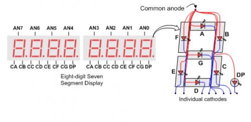
Across all eight digits, the ca segments of each are tied together for example, same with cb, etc... Therefore we are never able to apply a signal to a specific ca segment on any digit. However, since an LED only glows if the anode and cathode are the correct values, by setting this global ca to a value we want and then selecting which digits to activate by using certain an pins, we can at least control which ca pins on particular segments light up. The same logic applies for the remaining cathode pins/segments as well like cb, cc, etc...

Still, while we can turn off particular digits by varying which values on an are on and off, there is no way using only combinational logic that we could ever show two separate on two separate digits. If I needed to show the numbers 0000_1986 many of these digits are using different combinations of segments a through g and there'd be no way to do this with combinational only logic.
The question that should be jumping out to you is how do we make the different segments say different things at the same time if they're all tied together in this way? The answer is we don't. Or we sorta do, but it is complicated. What we can do with our LEDs is sequentially light up each of the eight digits with the appropriate pattern for its digit, while keeping the others off. If we do this fast enough (keeping each digit lit for something like 1 ms) and repeatedly for each digit, we can make it look like all eight digits are illuminated to our inferior human eyes.
This should seem possible to you. We have access to the anodes (which "activate" a given digit).
We put together a nice cartoon to show this concept a little bit more clearly:

ca pin, for example instead of having all of them share a common control pin. As it turns out, controlling the display by "strobing" each segment drastically cuts down on the number of pins. If we did it the brute-force way, you'd have eight pins per seven-segment display (one common anode, and seven cathodes), times eight segments, that'd be 64 pins needed. No thank you. Doing it this way requires only 15 pins. Pins equate to circuit board and chip real estate and this usually equates to money. As Method Man tells us, Cash Rules Everything Around Me(Us), so strobing LEDs is beneficial.Let's now build a module called seven_segment_controller which will be responsible for controlling all eight digits of the seven-segment displays. To make this module as functional as possible (for later usage) it will be responsible for displaying hex on all 8 digits, meaning it can represent 32 bits of information (4 bits per hex symbol) even though we're only using it for 16 in counting button pushes at first. Consequently, this module should have three inputs:
val_in[31:0]: a 32 bit input which will get rendered on the display (in hexadecimal)clk_in: An external system clock for driving the synchronous logic in the modulerst_in: a reset control in case you'd like to make your module resettable.
Additionally, the module will have two sets of outputs:
cat_out[6:0]: Pins intended to drive the cathode pins in our system.an_out[7:0]: Pins for selecting/deselecting the individual segments via their anodes (note, again, that driving high an anode disables a given digit)

For the initial deployment, we're counting button pushes. btn_count is only 16 bits, but the input to the seven segment module is 32 bits. As a result, the upper 16 bits of val_in will be default 0 and you'll only be able to control the lower four hex digits for this first demo; that's ok.
We're going to provide an almost-complete version of seven_segment_controller below. Study this code and get it working. It does not need much more to work like we just described...perhaps ten lines max. The missing piece is effectively to route the appropriate seven-segment pattern to led_out given the current digit being activated! (See the sequential image above and try to match what it has for values with the code below!).
This module is a very basic form of state machine, which we'll be covering in upcoming lectures/labs! Note that it uses an instance of bto7s from lab 1 so you should bring a copy of that into your project as well (you can either put it in a separate file or include it below in the same file)! Other than wiring everything together, this module should just work!
`default_nettype none

module seven_segment_controller #(parameter COUNT_TO = 'd100_000)
                        (input wire         clk_in,
                         input wire         rst_in,
                         input wire [31:0]  val_in,
                         output logic[6:0]   cat_out,
                         output logic[7:0]   an_out
                        );
  logic [7:0]	segment_state;
  logic [31:0]	segment_counter;
  logic [3:0]	routed_vals;
  logic [6:0]	led_out;
  /* TODO: wire up routed_vals (-> x_in) with your input, val_in
   * Note that x_in is a 4 bit input, and val_in is 32 bits wide
   * Adjust accordingly, based on what you know re. which digits
   * are displayed when...
   */
  bto7s mbto7s (.x_in(routed_vals), .s_out(led_out));
  assign cat_out = ~led_out; //<--note this inversion is needed
  assign an_out = ~segment_state; //note this inversion is needed
  always_ff @(posedge clk_in)begin
    if (rst_in)begin
      segment_state <= 8'b0000_0001;
      segment_counter <= 32'b0;
    end else begin
      if (segment_counter == COUNT_TO) begin
        segment_counter <= 32'd0;
        segment_state <= {segment_state[6:0],segment_state[7]};
    	end else begin
    	  segment_counter <= segment_counter +1;
    	end
    end
  end
endmodule // seven_segment_controller

/* TODO: drop your bto7s module from lab 1 here! */
module bto7s(input wire [3:0]   x_in,output logic [6:0] s_out);

endmodule // bto7s

`default_nettype wire
seven_segment_controller, rst_in. It is almost always a good idea to give your sequential circuits a reset signal both for regular operation but also for debugging since it can give you the ability to get your circuit back to a known starting state.
When the above code is working, update seven_segment_controller.sv. Make sure to uncomment the instantiation of the seven_segment_module in the top_level file and delete any unneeded lines. Build, and upload. Hopefully you're getting a video like below! If so, get the checkoff!
HERE is a video of the seven_segment_controller working
When you have assembled all these pieces, show to a staff member for the seccond lab checkoff. Note, if you move onto the next section, you can get still get checkoff 1 by default since it will include the functionality shown here. It is up to you if you want to get this one now or merge them in the next section.
Before the era of USB, keyboards and mice would communicate with their host computers over a protocol known as PS/2. This is a relatively simple protocol that communicates keystrokes or mouse movement/clicks with relatively low latency.1 The Nexys boards we use have a small microcontroller onboard that converts USB signals from modern keyboards and mice back to PS/2.
Since the PS/2 protocol is nice and simple, we'll have you build a PS/2 decoder in this section. Once that's done, we'll connect its output to the seven-segment display through a shift buffer, and you'll be able to see the onboard display change as you press the keys!

PS/2 works by representing each character on the keyboard as a one-byte value from a predefined table, and sending that across the interface when a key is pressed.
Whoa whoa whoa, what does "sent" mean?
Basically, the PS/2 protocol runs over two connections / 'lines' between the device (i.e. your keyboard) and the PS/2 controller. The first of these connections is a clock, driven at a few kilohertz2 by the keyboard. The second of these connections is where the actual data flows. When the clock line drops from high to low, we can grab the value of the data line and store it for later use - eventually stacking up a full eight bits of information. This byte of information corresponds to a "scancode" in the above table, which maps to the character that you just pushed on your keyboard. However, as is often the case in communication of data, more than just the message must be sent in order to avoid ambiguity.
The transmission of an entire byte, therefore looks like the following: When you press down a key (or release a key...see below), you're gonna see the following happen:
- The clock line, which is high at idle time, is going to start ticking at its frequency of a few kilohertz. Meanwhile, a start bit, which signals the beginning of the transmission (and is always zero), is asserted on the data line. So at the first falling edge of the clock in a given sequence, you're going to see a 'zero' value asserted on the data line.
- The next eight falling clock edges will bring along 8 data bits, which contain the byte that represents the key you pressed.
- Next you'll see a parity bit, which is used for error checking. This uses the same method as you saw in pset 03. PS/2 uses odd parity which means if there are an even number of 1's in the 8 bits of the actual message a 1 is in the parity bit slot. If not, then a 0 is in the parity bit slot.
- Finally, you'll see a stop bit which is always a one. This signals the end of the transmission, and its receipt corresponds with the last falling clock edge you'll see until the next key is pressed.
For you visual folks, here's a quick diagram summarizing the above.

We're going to put together a module that decodes the PS/2 signal from the clock and data lines. We've provided the framework for you below, but your module should include:
clk_in: The system clockrst_in: A system resetps_data_in: The data line of the PS/2 inputps_clk_in: The clock line of the PS/2 inputcode_out: The 8-bit scancode from the keyboard.code_valid_out: A signal that goes high when a new code has been decoded from the interface (and it passes parity check). It should remain high for only one cycle of the system clock before being reset to zero.
Good luck with this! A few helpful points about stuff you might observe along the way:
- PS/2 doesn't just send keypresses - it also sends other information about the state of the connected device at a given time. Most notably, whenever a key is released, the keyboard will send over the byte
0xF0, and then the scancode corresponding to the key you pressed. For this reason, it's common to see patterns likeXY F0 XYin your testbench and on your 7 segment display, whereXYis a scancode of a given key. - If you hold down a key, you should see the same scancode repeated over and over again!
- Not that it matters to you, but PS/2 was/is used for mice too!
We've included a partial checker for your ps2_decoder below. It is worth 0 points since it only tests for some functionality; it does NOT test for all needed functionality, specifically for if/when code_valid_out fires or not since that can be quite variable depending on your implementation. 100% here may suggest it'll work on the board, but does not guarantee it. We're also providing a ps2 testbench for your local debugging. You should definitely be using the waveform analyzer for debugging this module!
Once you're done with the above, great job! We can now integrate this into hardware. To do so, proceed with the following steps:
- In
top_level.sv, make sure that you're feeding the contents ofps2_bufferinto the seven segment controller. You probably left this commented out earlier - go ahead and swap it for your counter's output. - Next, you should add a small shift buffer to the bottom of your top_level.sv. Whenever
ps2_validis asserted, i.e. wheneverps2_codeconsists of a valid code received, you should shift this code into the least significant byte in theps2_buffermemory - shifting all other values to the left and knocking out the least recently received byte. - Build using your preferred method and see what happens!
The video link below is an example PS/2 implementation working as expected. Your solution should look like this!
HERE is a video of the PS/2_controller working
Show your system working!