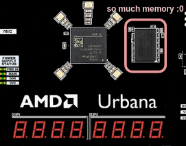
Checkoff 01: HD Camera
Look at all those pixels
Please Log In for full access to the web site.
Note that this link will take you to an external site (https://shimmer.mit.edu) to authenticate, and then you will be redirected back to this page.
Last week, we had our cameras giving us 1280x720 pixels of data for every frame, but we had to cut it down to a much smaller size to fit it all into our BRAM frame buffer. Pretty unsatisfying, right? Down-sampling by four in each direction means we actually were only showing one-in-sixteen pixels from the camera. Blah. Today, we're going to fix that problem! Your design for this week will start from a basis of what you had last week, and swap out the frame buffer BRAM for a data pipeline that can stick our camera feed into a much larger form of memory, the off-chip DRAM!
To get started, make a copy of your week05 final camera design: you'll need much of the data pipeline, but especially the center_of_mass module; we'll make some great use of it in the second half!
Then, download a handful of files. Some of these are new, but the top_level should replace your last-week top_level.:
- base.zip: HDL files, which includes:
top_level.svwhich is very similar to last week, but hooks up all the new modules we'll need in order to interact with the DRAM. It skips the data pipelining you added: you don't need to worry about properly pipelining and removing artifacts this week. You will need to add your susbampling and scaling logic back in!stacker.svandunstacker.sv: deserializes and serializes pixel data to be written/read as 128-bit messages.traffic_generator.sv: A partially finished generator of commands for the memory controller, which you'll add finishing touches to to write and read camera data to the memory chip.high_definition_frame_buffer.sv: The top-level connections for the full data pipeline feeding data in and out of our memory chip. You'll make finishing touches to a few signals in this file as well.clockdomain_fifo.sv: Wrapper to a Xilinx-built FIFO that can handle clock domain crossingddr3_top.sv,ddr3_phy.sv,ddr3_controller.sv: The UberDDR3 IP core that will serve as our memory chip controller.lab06_clk_wiz: An additional clocking wizard to generate the clock speeds our memory controller will need.
- top_level.xdc: Similar to last week's, but with the addition of the
ddr3_*signals to connect to our memory chip. We'll need to use everything that was in the week 5 system, since we're augmenting that system directly; so, bring over the files you wrote to build up your video pipeline! (pixel_reconstruct, center_of_mass, etc.)
Don't forget to bring in the files in your data folder! Especially your rom file(s) for configuring the camera!
SUMMARY: In your new top_level:
Copy in your camera subsampling and 4X scaling logic from your week5 top_level. You can remove the 1X and 2X scaling modes now: just copy in the scaling logic from each row. If you previously were flipping your horizontal coordinates (e.g. by determining a coordinate 319-hcount) you shouldn't do this now, as the DRAM frame buffer pipeline won't be doing this mirroring.
Starting this week, we're building some really hefty piece of "IP" alongside our own designs. The process of synthesizing the UberDDR3 memory controller is much higher effort for Vivado than our past little chill Verilog designs, so your build times will get longer this week (a good, working build will take ~two minutes). That means it's worth it to try and catch typos/syntax errors without having to wait through a full build!
Side-stepping the BRAM

Getting things into and out of the off-chip memory is way more complicated than using the nice, friendly BRAM blocks inside the FPGA fabric. If we tried to do it all from scratch, we'd be be fighting a seriously long and drawn-out battle. Luckily, its a problem that many before us have worked hard to solve. Xilinx provides an IP (intellectual property) core that can serve as our memory controller, but it uses a lot of resources, so instead we'll opt to use an open source IP project, the UberDDR3 memory controller, written and documented by a very talented engineer. This project handles all the upkeep the DRAM chip will require, and read and write from addresses as we request from it, as well as providing a reasonable interface we can communicate with.
Of course, by introducing this memory controller, we've just replaced the problem of "how do I work with a memory chip?" with the problem of "how do I work with the memory controller?" It's a better problem to have, but we'll still need some infrastructure in order to set it up properly. There are a couple major constraints of working with the memory controller that we'll need to design around:
-
Clock Speeds The spec of the DRAM chip demands that we run it somewhere in the 300-400MHz range, and our specific memory controller configuration has it running at 333.333MHz. There are 16 parallel data wires between the FPGA and the DRAM chip, so 16 bits of data are sent at a time. Since the chip is DDR, or Double Data Rate, we can send data on the rising and falling edge of that clock, so we can send 16 bit messages at an effective rate of 666.666MHz (the clock cycle of the beast). That's really fast--probably too fast for the logic we'd write to send messages to the DRAM. So we use a clock that's 4 times slower than the chip's operating clock, of 83.333MHz. We need to give the controller data on this
clk_controllerclock. -
Data Width Since we're operating at this clock that's 4 times slower than the DDR chip, the memory controller can send more messages on the 16-wide bus each clock cycle. Specifically, since we feed it data at 83.333MHz and it can double pump data at 333.333MHz, there are (4*2) = 8 chances to send a 16-bit message between each controller clock cycle, so it wants us to give it 128-bit messages on each cycle.
Now these constraints are annoying, considering we have two other clock speeds we need to produce and consume data, and each of our pixels needs 16 bits of storage, not 128. But we have tools at our disposal to surmount these challenges!
Stacking, Unstacking, and FIFOs
In order to get data into our 83.333MHz controller clock domain, we need something that carries our data from one clock domain to another. For that, we'll use a FIFO structure provided by Xilinx; unlike the FIFO you just wrote, it can handle the task of crossing clock domains. We'll write data on one side of the FIFO in one clock domain, and we'll read data on the other side of it in another clock domain. This is both how we'll get pixel data into the controller clock domain from our pixel reconstructor, and how we'll get pixel data from our DRAM frame buffer to the video pipeline and HDMI output. We can trust that the clock domain crossing is being handled appropriately inside of the Xilinx structure.
Using a FIFO here also lets us worry less about the exact timing of the DRAM. Sometimes a request to get memory from the DRAM chip could take 30 clock cycles, and sometimes it could take 300, but that manifests itself only as the FIFO being more or less full at individual moments. As long as the average time it takes to acquire the data we need is less than how much data we need to consume in a given period of time, the FIFO should keep us covered!
Our FIFO, like the memory controller, will deal in 128-bit messages. In order to accomodate getting data into and out of these FIFOs, we've also provided you with two modules: a stacker and an unstacker. The stacker takes sequential 16-bit messages and stacks them into one larger message, and adds a message to the FIFO when a full 128-bit message is ready. The unstacker does the inverse--it takes a 128-bit message out of the FIFO and serializes it into 16-bit messages.1
All three of these components, the FIFO, the stacker, and the unstacker, speak to one another and to you using AXI-Stream, which is discussed in depth in Lecture 11.
AXI-Stream: Bursts of transactions
AXI-Stream is a protocol by which we can carry data between two modules, and completely specify unambiguously when data is actively being transferred (if followed, no data samples should ever get "dropped" in AXI). Many of the modules you've already written have used some version of a ready and a valid signal; one of the most valuable things that AXI-Stream provides us with is a way to formalize that! And since the FIFOs, stackers, and unstackers rely on this protocol to understand our requests. You need to properly set your tready, tvalid, and tlast signals to tell these modules what you want to be doing with your data. These three signals together enable the unambiguous handing off and characterization of our data.
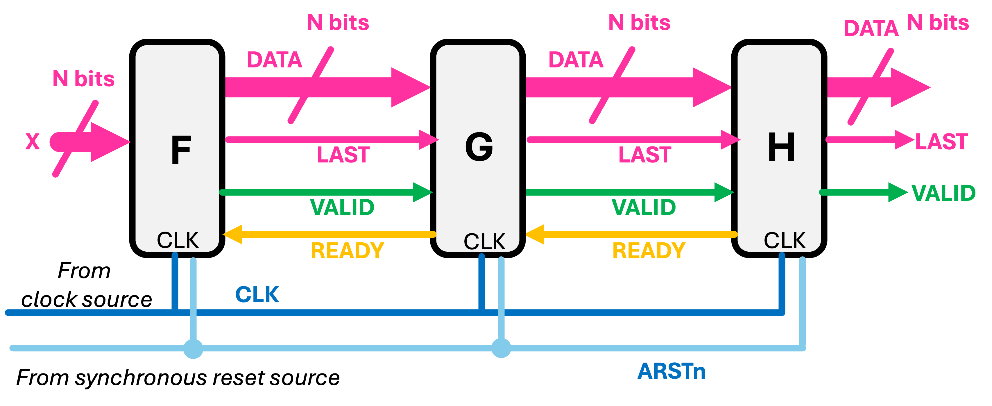
Make sure to review lecture where the meaning and purpose of READY/tready and VALID/tvalid are discussed. This is important.
When streaming data over AXIS (AXI4-Streaming), only the data gets sent. Unlike with more complicated versons of the AXI protocol (like Full AXI or AXI-Lite), there is nothing such as address values that are sent along with the data. As a result, the order of the data is very important and specifies where/when a particular datum "lives". Furthermore since we'll often be sending a set of data, and then want to send a different set of data, so we'll need the ability to specify the "boundary" between those different sets so things don't flow together incorrectly. That's the purpose of a LAST/tlast signal; It can allow the long sequence of pixels we're sending to our FIFO to have an accompanying alignment marker.
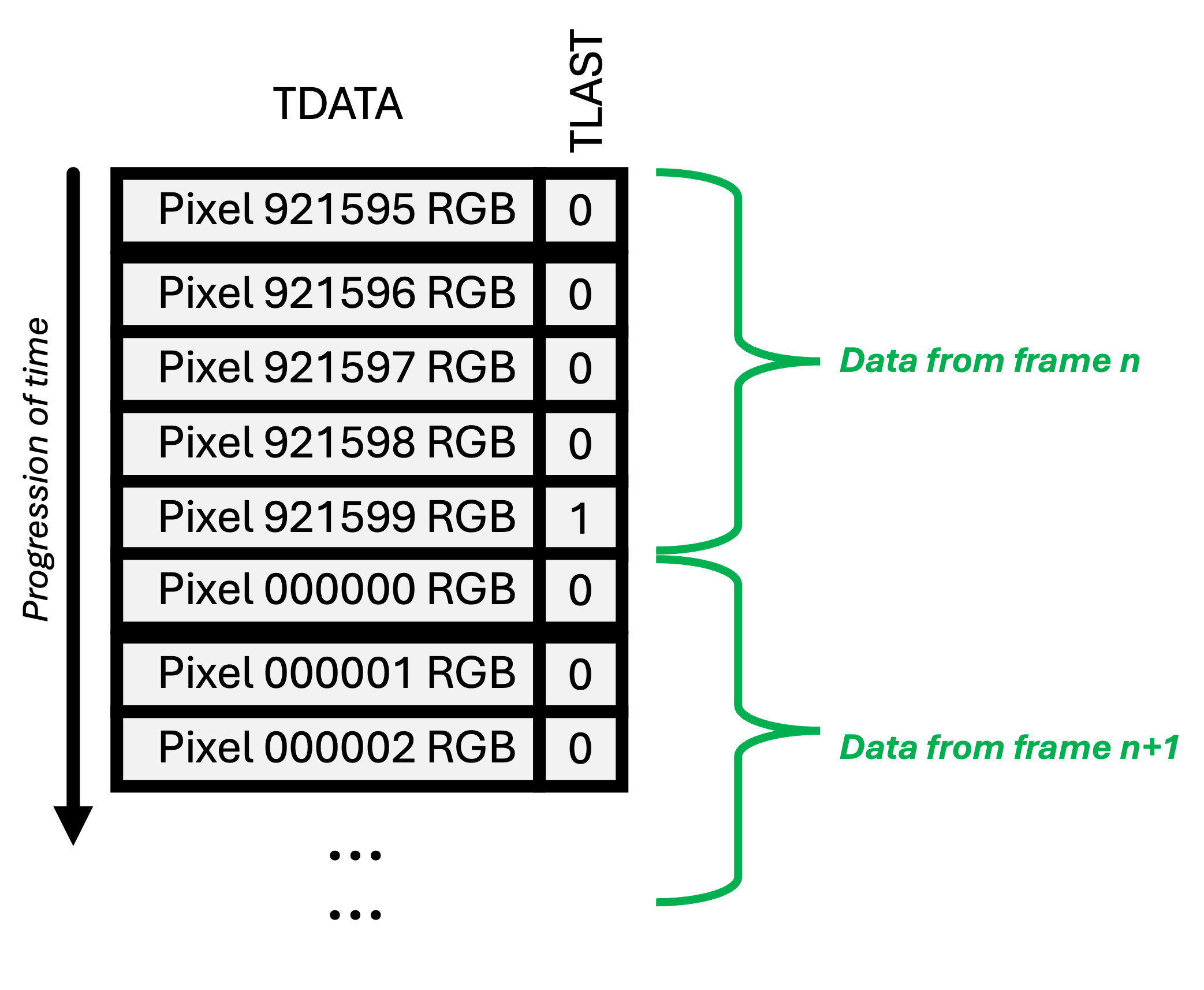
The tlast signal is a single bit, that we want to set high when we're transferring the last pixel in our frame buffer: aka, the bottom right corner of the camera feed. It accompanies that piece of data as it flows through the system. There are a couple places at the that we need to specify and interact with the tlast signal to properly generate an output (both of which should be added to your high_definition_frame_buffer.sv module):
-
TLAST into Stacker: When passing camera data into the DRAM buffer, we need to indicate where a new video frame starts and ends. We need to generate a
tlastsignal at the output of our pixel reconstructor/input to the stacker. This should be a pretty simple piece of logic, that uses thehcountandvcountvalues from your pixel reconstructor to only be high when we see the bottom right corner of our camera feed. -
TREADY into Unstacker: We need to properly react to a
tlastsignal on the output of the unstacker, when we're receiving our frame buffer. Specifically, we want to use it to help interpret whether or not we should have ourtreadybe high. So let's think more completely about how to lay out thattreadylogic!
The data pipeline we're using here has a FIFO that we can rely on always having some amount of data in it. So, we can expect that the tvalid signal out of our unstacker will always be high, but we only sometimes actually need to consume a pixel out of this stream of data; other times, we might be busy hsyncing or vsyncing in our HDMI output signal. Every cycle where tvalid and tready are both high is a successful ready/valid handshake, or a cycle where the stacker will think you've listened to it and sent a pixel on its way to be drawn on the screen. So you should only let tready be true if you actually are sending a pixel to be drawn on the screen. If you "lie" to the stacker, and don't store it when you said you got it, you're out of compliance.
If you see that the tlast signal coming out of the unstacker is high, but you're not about to draw the pixel in the bottom-right corner of the screen, you know that something is out of sync. What can you do about this? You can wait until things are right again! If your tlast signal is high and you're not about to draw the bottom-right corner of the screen, you can make your tready stay low, which makes sure that the pixel you need to draw in the bottom-right corner will stay in place in the unstacker until it's actually time to be true. So, if you see a tlast signal, your tready should only be true if you're drawing the bottom-right corner.
Write a piece of (combinational) logic that defines the tready signal output
frame_buffer_tready signal, based on the values of active_draw_hdmi, frame_buffer_tlast, hcount_hdmi, and vcount_hdmi. If you're not sure how to write out that expression, talk to a friend or a staff member about it.

SUMMARY: In your high_definition_frame_buffer file:
- Fill in the logic indicating how to generate a tlast for the burst of reconstructed pixels
- Fill in the logic of what your
treadysignal should be at the output of the unstacker, when you receive your pixel values.
Generating Traffic (You Are the Traffic)
Now that you've laid out the AXI-Streaming signals to get data in and out of our clock-domain crossing FIFOs, the only piece remaining is specifying the commands that will be issued to the UberDDR3 memory controller. That's where our traffic_generator module comes in; it connects to the FIFOs that feed in and out our camera data, and defines the signals that the memory controller interprets as read and write commands. As such, it has to be equipped to handle the ready and valid signals of our data FIFOs, as well as the busy-indicator signals from the UberDDR3 modules.
Most of this traffic generator is already written for you: it has a state machine that alternates between issuing read commands and write commands, whenever each is available. And it sets the signals for the FIFOs it's connected to to indicate when it actually consumes a message from the input FIFO with a tready signal, or writes a message to the output FIFO with a tvalid signal. The part you need to add in is a way to determine the address that should be associated with these commands.
Address Counting
There are two addresses in memory we need to keep track of:
write_address, The memory address that the next piece of data consumed from the write AXI-Stream FIFO needs be written into. This should increment every time a ready/valid handshake happens with the write AXI-Stream FIFO, and should reset every time there's a ready/valid handshake wheretlastis high.read_request_address, The next memory address that we need to submit a read request for in order to read out the FIFO in order. This doesn't have an AXI-Stream associated with it (since theread_axisis what we output when we get a response), but we've defined aread_request_validandread_request_readypair of signals, such that the event of both signals being high indicates a successful read command submitted.
I wonder if we might have a friendly little module sitting around somewhere that does a great job at counting, events? Oh I don't know, maybe an evt_counter? Make sure you use the version of your evt_counter that specifies a MAX_COUNT, so you can make your address loop back around when it reaches the end of the frame buffer. Set up some event counters that count ready/valid handshakes that happen on each of these AXI-Streams!
Again!!!...Make sure that you are using the evt_counter you created that can count up to an arbitrary number and which does not need to rely on natural overflow! This is very important! Also note that you may need to modify the size/capacity of your evt_counter to work as you need for this lab! (16 bits may not be enough).
Tracking commands while we wait, with a FIFO
Once you've specified the addresses for read and write commands, you'll need a way to track the commands that are still in-progress, or "in-flight." The memory controller can take many commands in sequence, and will return its response data in the order you issued commands, but the latency from issuing a command to getting a response can be large, and can vary greatly! If you're lucky, your read request might be done in 15 clock cycles, or maybe the DRAM chip will be busy getting refreshed and it'll take 350 clock cycles, or maybe it is immediately able to write and does it in a clock cycle (unlikely but let's not assume). So, we want to use a FIFO that writes down every command we send in, and read what command we're getting a response for when we get a value out. Luckily, this is exactly what we just designed our command_fifo to be from the previous assignment/first checkoff.
In order to keep track of our commands, we'll want each entry in our FIFO to store both the address we're writing to, and the bit indicating whether we're reading or writing. Those signals will need to get concatenated together, and then separated into their appropriate signals again at the output. We'll want to write down those values whenever a command enters the memory controller, which is true on any cycle where our enable signal is high and our busy signal from the memory controller is low. Our command_fifo should be written in such a way to display the next available logged command to be read (why we made it have asynchronous readout of its memory). In order to mark down that we've "used" the logged command, we'll want to read our response when we see the memrequest_completed signal go high, indicating the first-out command in our FIFO has finished. In steady-state, this should then move the read pointer up in memory space, allowing the next logged command to be available for reading in the future when the next DRAM memrequest_completed signal comes back.
Finally, once we've gotten values out of memory and we know they were responses to read requests, we'll need to make sure to frame them appropriately with tlast signals. You'll need to use the read_response_address coming out of the FIFO to determine when the tlast signal for our output FIFO should go high. When we're transmitting the final 128-bit chunk of our frame buffer, we should set the tlast signal high.
read_response_address should indicate that our read_axis_tlast signal should go high?
_SUMMARY: In your traffic_generator, add:
- Two event counter-type modules to specify the addresses we associate with write reqeuests, read requests, and read responses.
- A
command_fifowith depth 64 that stores the command address and write_enable signal every time a command is issued to the memory controller, and reads an item out whenever thememrequest_completedsignal comes back from the memory controller. - A definition of the
tlastsignal, based on the address that has most recently come out of your FIFO.
Debugging this stuff in hardware can really suck. Your build times take 2-3 minutes now, and it's hard to determine where in this whole pipeline your error has come from by looking at a garbled camera output. If you're stuck, Write a testbench for your addressing evt_counter, and make sure you're confident about the events that define your addressing! Additionally, go back and confirm the behavior of your testbench from your command_fifo. If a staff member gets called over to help you and you don't have a testbench to help us help you, you'll be dropped from the queue and will need to write one.
A Completed Data Stream
At this point, you've fully hooked up the addressing that needs to be done to set up your data pipeline! Switch your sw[0] to 1, and if all your addressing and AXI-Stream signals are configured properly, you'll see your camera output in the true 720p quality it was destined to be! Flip back and forth between your subsampled BRAM buffer and the DRAM buffer--really take it in. A thing to look at switching between the two modes is text (like on your phone or a piece of paper). The 2D spatial frequencies of text are high enough that when improperly downsampled (as we did last week) without anti-aliasing filtering, you can get really bad looking stuff. At full resolution, things should be ok enough.
Show a staff member your full-quality image buffer! Be ready to discuss:
top_level.sv for staff review.
high_definition_frame_buffer.sv for staff review.
traffic_generator.sv for staff review.